Test department of PREMA Semiconductor GmbH
The test department has an automated wafer tests and handling systems that enable to test all wafers and ICs based on required and agreed test conditions. 100% of the products are tested and defect ICs are automatically selected.
Each prober and handling systems has an individual test system that has been developed and produced by PREMA to meet highest needs in flexibility and economy. The calibration of the measurement devices is done frequently using standards of the Physikalisch-Technischen Bundesanstalt (PTB) located in Braunschweig.
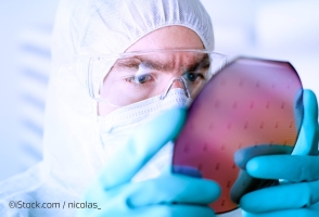
We optically and electronically inspect all wafers that leave the production line. Using standardized test structures, additionally applied to each wafer, we check all basic parameters. Afterwards, the wafers are exposed to further tests that are individual for each IC.
On a wafer, all ICs are tested first by our quality department. The IC test bases on a procedure that is set by PREMA and your experts. ICs that drop out are marked to be separated later on. Occasionally, voltage references or other circuit blocks can be trimmed at the same time.
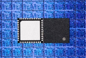
Afterwards, tested wafers are sawn, bonded and encapsulated. All common PDIP, SOP and SSOP packages are available. Other package types can also be offered upon request (g.e. Flip Chip). To complete the production cycle, all encapsulated parts must pass another complete IC inspection, before the final shipment to you is initiated. Additional test procedures, such as burn-in, are available on demand. Encapsulated Chips (ICs) can be delivered in tubes or with tape on reel.
Tested wafers can also be delivered as produced, grinded, sawn on tape, sawn on tape with expander ring or in waffle pack.


